
imec announces a single exposure of High NA EUV microfilm technology, promoting the development of process below 2 nanometers
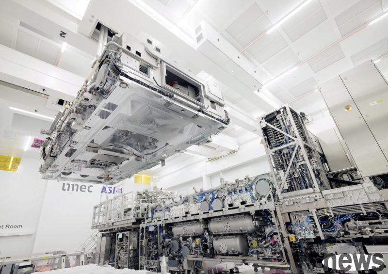
The Belgian Microelectronic Research Center (imec) recently released a major news, announcing that it has achieved a new breakthrough milestone in the single-time graphics technology of high-number pore ultraviolet exposure (High NA EUV), representing the strong strength of the High NA EUV graphics capabilities to A10 and more advanced logical stages. At the same time, it has also emphasized imec's leading position in the field of exposure as the research and development of film technology.
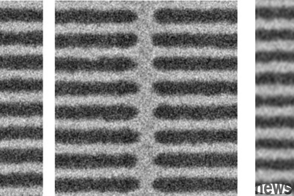
The results were publicly displayed at the 2025 SPIE Photomask Technology + EUV Lithography Conference, including two key breakthroughs. First, in the process related to damascene metallization, a 20-nanometer-distance structure was successfully realized, and its tip-to-Tip (T2T) boundary dimensions (CD) reached 13 nanometers. Secondly, through Direct Metal Etch (DME) process, the electrical performance test results of the Ru line were obtained.
At the 13-nanometer T2T dimensional structure achieves industry milestone, Imec has demonstrated a 20-nanometer-distance metallization line structure at the SPIE Advanced Exposure and Graphicization Conference in February 2025. On this basis, Imec has successfully achieved a 20-nanometer-distance linear structure through a single exposure High NA EUV exposure step, and reduced the borderline size (CD) from tip to tip (T2T) to 13 nanometers.
In these 13-nanometer T2T structures, the measured local CD uniformity (LCDU) is as low as 3 nm, a data that is considered an industry milestone. Steven Scheer, Vice President of IEC Computing System Expansion, pointed out that using single exposure High NA EUV exposure technology to achieve these logical designs, compared to multi-patterning technology, can reduce processing steps. This advantage directly brings multiple benefits to reduce production costs, improve yields, and reduce environmental impacts.
▲ Major achievements highlight the strength of the imec High NA EUV ecosystem in promoting High NA EUV patterning technology to A10 and higher logical points.
These links support the industry standard of interconnected manufacturing - damascene metallization. T2T zonal structures are an integral part of the interconnection because they allow for intermittent metal tracks. In order to meet the logical process blueprint requirements of 20 nanometer metal distance, the T2T boundary dimension distance must be reduced to 13 nanometers or less, while still maintaining the performance of functional interconnections.
At present, imec is continuing to develop to further reduce the T2T size and has achieved good development results in the 11-nanometer T2T boundary size. In addition, the relevant structure is working to move into the lower layer hard mask to achieve a true (dual) embedded interconnection. To achieve these results, Imec used metal oxide resist (MOR) and was co-optimized with the base layer, illumination pupil shape, and mask selection.
Then in terms of the high yield interconnection of direct metal etching (DME) and the spiral circuit, as the industry advances to metallization processes below 20 nm, the industry may need to turn to alternative metallization solutions. As the second major achievement of imec, they demonstrated the compatibility of the direct metal etching (DME) technology of the squid (Ru) with the single exposure High NA EUV exposure technology.
Through DME process, imec successfully achieved a 20-nanometer and 18-nanometer distance line, including a 15-nanometer T2T boundary dimension structure. These results also include functional interconnections with low resistance. It is worth noting that for the metallization wire structure at a distance of 20 nanometers, ICP has achieved a 100% electric performance test yield.
imec's significant achievements benefited in part from the support of the NanoIC pilot line in the EU. These results not only mark the important progress in the single exposure capability of High NA EUV, but also highlight the key role of the cooperation between Imec and ASML. This partnership is important for promoting a more extensive ecosystem, which is driving the transformation of High NA EUV to high-volume production, thereby unblocking sub-2nm (sub-2nm) logical blueprints.
Steven Scheer mentioned that since the launch of the ASML-imec joint High NA EUV laboratory in Veldhoven, the Netherlands, Imec and its partners' biotechnology system have made significant progress in developing High NA EUV exposure and pushed the industry to the angstrom era. In addition, the results displayed by imec mark a new milestone, once again confirming the leading position of imec in the field of exposure research and development. These achievements have a key role in achieving the European Chips Act's goal of promoting the process of logical sessions below 2 nanometers..
imec's close cooperation with ASML High NA EUV ecosystem includes leading chip manufacturers, equipment suppliers, material and photoresist suppliers, mask companies, and measurement experts. Through joint optimization with these partners, Imec will continue to support the progress of logic and memory process blueprints.
Recommend News
-
Cambrian became the king of Chinese stocks, with a price-to-earning ratio of 595
-

Winbond s profit in September increased by 317.29% year-on-year, and EPS reached
-
Korean media: NVIDIA stops SOCAMM reopens design, Micron first develops its adva
-

Ximen launches new smart verification solutions to accelerate verification proce