
From EUV to new photomask technologies, see how Zeiss Semiconductor is co-creating the future of chips with Taiwan
As TSMC is about to enter the era of 2-nanometer mass production, ASML’s EUV lithography machine is regarded as the key to process advancement. But you may not know that even as powerful as ASML, you still need a strong partner to make the most cutting-edge technology possible.
This partner is the German optical giant Zeiss Semiconductor.
ASML can accurately project extreme ultraviolet light (EUV) onto silicon wafers, thanks to the lens module created by Zeiss Semiconductor, which is claimed to be the most sophisticated lens module in the world. Without Zeiss’ breakthrough in extreme optics, ASML’s EUV equipment would not be able to accurately depict billions of transistors on the wafer. Zeiss Semiconductor is the indispensable "heart" in this semiconductor revolution led by ASML.
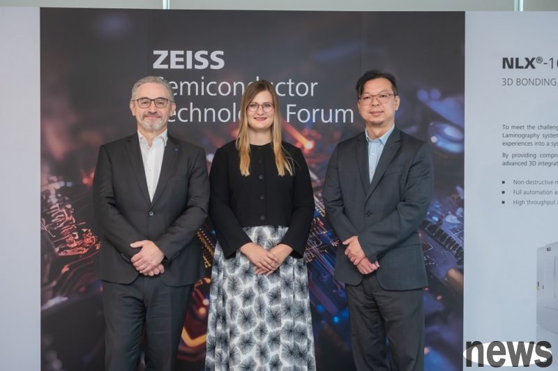
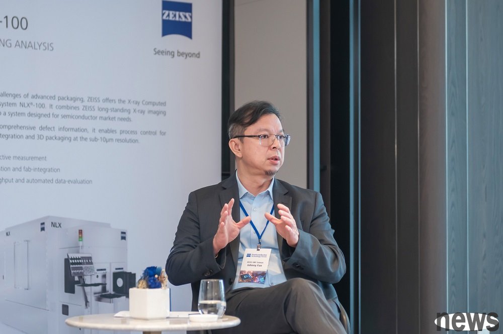
This time, "Science and Technology News" had the opportunity to meet three soul figures of Zeiss Semiconductor face to face at the 30th anniversary semiconductor event of SEMICON Taiwan: one is Dr. Thomas Stammler, chief technology officer of Zeiss Semiconductor, the other is Fan Yaliang, general manager of Zeiss Semiconductor Taiwan, who is deeply involved in the Taiwan market, and Jeannine Rapp, head of media public relations of Zeiss Semiconductor. They not only revealed Zeiss Semiconductor's latest layout in EUV and mask technology, but also shared why Taiwan is a key strategic place in this global technology competition.
The driving force behind the wave of AI has already quietly laid out the photolithography technology for the next 10 years.This exclusive interview starts with the core technology provided by Zeiss in the semiconductor industry, which is the lithography optical technology in EUV. EUV devices are key to the continuation of Moore's Law to this day and are the cornerstone of current AI development. All high-performance AI chips are inseparable from the blessing of EUV lithography technology.
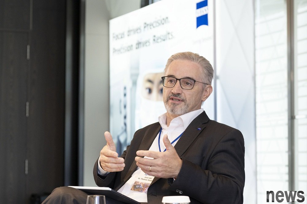
Thomas compared Zeiss Semiconductor’s EUV development to a 30-year “technology marathon.” He said: "We started the development of EUV 30 years ago, including the lithography optics used in EUV lithography equipment. We have worked closely with our strategic partner ASML for more than 30 years and accumulated a lot of experience. For such a technology, it is not a sprint, but a marathon."
What are the advantages of Zeiss Semiconductor? Thomas bluntly said that to be a champion in a certain field, you must cooperate with champions around the world, and this is exactly what Zeiss Semiconductor is doing. In addition, there is Zeiss’ commitment to innovation, which is also the key to enabling Zeiss Semiconductors to continue and stably provide customers with leading technologies and ensure that customers can rely on Zeiss Semiconductor solutions for decades.
However, this marathon is not over yet. Zeiss Semiconductor is not only bringing a new generation of high numerical aperture EUV (High NA EUV) lithography products to the market, Thomas shared that Zeiss Semiconductor has already begun to invest in the research and development of the next generation, because the complexity of EUV equipment technology is very high, and the development time required for one generation is as long as 10 to 15 years, which means that Zeiss has begun to prepare for the semiconductor technology blueprint after 2030, 2032, and even 2035.
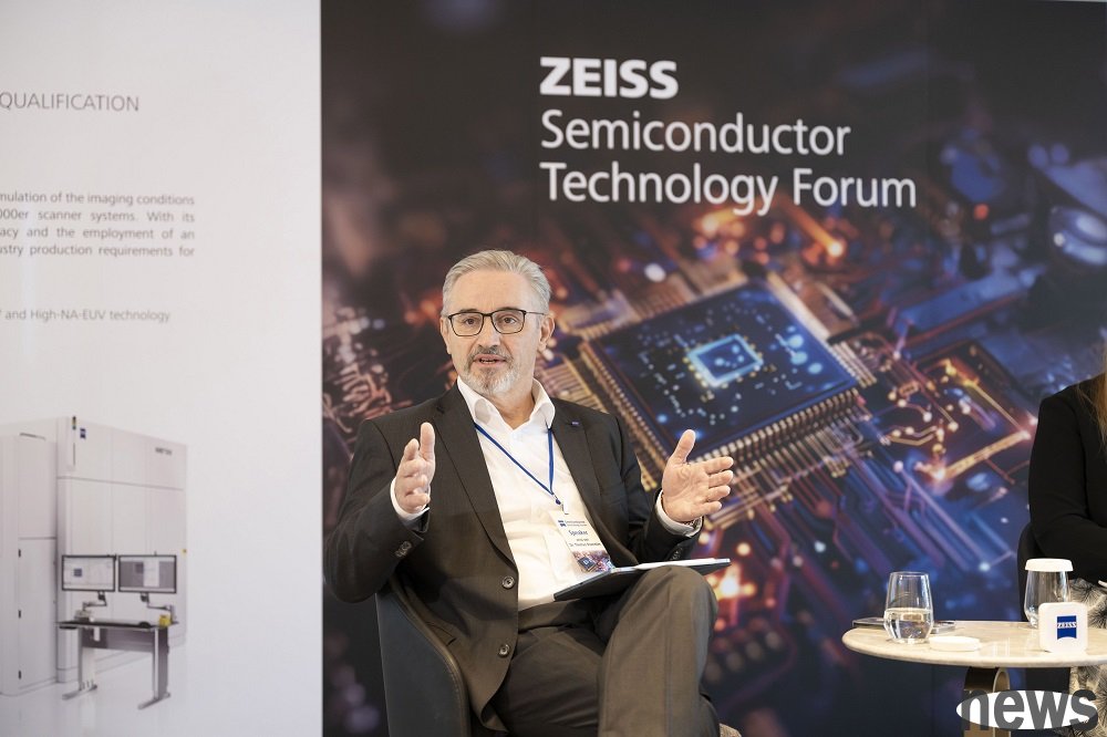
▲ Zeiss has established EUV optical advantages with a 30-year technology marathon. It not only drives AI chips and the continuation of Moore's Law, but also plans ahead for the semiconductor future of 2035. (Source: Science and Technology News)
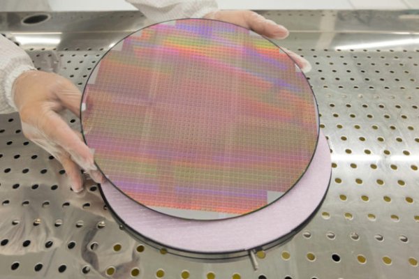
The key film for wafer manufacturing, pursuing zero defect in photomaskIf EUV lithography is a large camera that drives the AI chip, then the photomask plays the role of a "key negative." Any tiny defect on the photomask will lead to defects developed on the wafer, which will reduce the yield of expensive wafers. Just imagine, with the advent of the 2nm era, the price of a wafer is estimated to be US$30,000 (approximately NT$900,000). As long as the yield rate is reduced by 1 percentage point, the wafer factory will suffer considerable losses.
Therefore, "zero defects" in photomasks is not only a technical goal, but also a core requirement of customers.
"In order to support high yield in the manufacturing process, customers must have a very good, I would say, perfect mask, including perfect structure and perfect zero defects." Thomas said.
The reason why Zeiss Semiconductor has been a leader in the field of mask inspection and repair for many years is precisely due to its profound accumulation in lithography technology. Zeiss Semiconductor applies its 50 years of experience in optical design, manufacturing and R&D to all aspects of the photomask. They provide a complete set of photomask solutions, covering the complete process from measurement, correction, repair to verification.
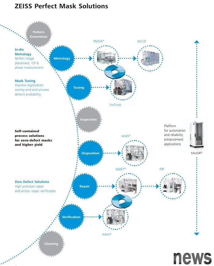
▲ Zeiss Semiconductor’s secret weapon to create “perfect masks” is a complete mask solution from measurement, correction, repair to verification. (Source: Zeiss Semiconductor)
This solution includes interlocking technical services, including Zeiss Semiconductor’s PROVE mask alignment and overlay measurement system. This system measures pattern positioning with sub-nanometer level repeatability and accuracy to ensure the correctness of pattern position.
In terms of mask calibration, ForTune helps chip manufacturers meet the most stringent specifications, using laser processing to improve mask critical dimensional uniformity (CDU), mask registration, and wafer product overlay (On-Product Overlay, OPO)..
In terms of mask repair, Zeiss Semiconductor provides MeRiT’s optimized solution. This solution is suitable for all types of mask repair and can repair the smallest defects. There is also a particle removal system (PRT) that can remove tiny foreign particles on the photomask.
On the verification platform, AIMS® EUV has the ability to verify the quality of the photomask and confirm whether there are critical defects on the photomask. In the interview, Thomas specifically mentioned Zeiss Semiconductor’s latest generation AIMS® EUV 3.0, which not only triples the mask measurement speed, but also has the advantage of being shared with the existing Low-NA-EUV.
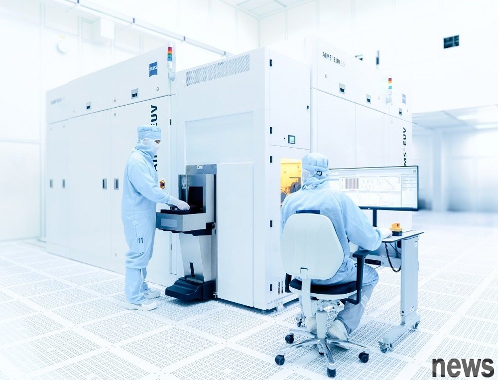
▲ Aiming at the new generation of High-NA-EUV, Zeiss Semiconductor has launched the latest AIMS ® EUV 3.0 system, which can measure masks three times faster and can switch between low numerical aperture (Low-NA) EUV and high numerical aperture (High-NA) EUV. (Source: Zeiss Semiconductor)
Fan Yaliang further explained that AIMS EUV 3.0 can switch between low numerical aperture (Low-NA) EUV and high numerical aperture (High-NA) EUV in a short time through software settings. This allows customers to avoid repeated investments and one device can cope with future technological evolution. As for customer feedback? "Very good!" Fan Yaliang replied with a smile. And his answer indeed reflects customers' high demand for technical efficiency improvement and cost control.
It is the joint assistance of these technologies that improves the quality of masks from DUV to EUV and the production yield of wafer fabs, echoing the "perfect mask" goal proposed by Thomas. Through these closely coordinated tools, Zeiss Semiconductor has not only become a promoter of the most advanced semiconductor processes, but also provides semiconductor manufacturers with solutions that combine production efficiency and yield benefits.
▲ Zeiss Semiconductor ensures "zero-defect masks" with complete photomask solutions, which not only improves wafer yield, but also allows customers to usher in the 2nm and High-NA-EUV era with higher efficiency. (Source: Science and Technology News)
Join hands with Taiwan to define the future of semiconductorsThese optical-based technologies and solutions are undoubtedly the solid foundation for Zeiss Semiconductor to gain a foothold in the semiconductor industry. But for Zeiss Semiconductor, this technological journey never stops at the technology itself.
At the end of the interview, Thomas and Fan Yaliang both emphasized that Zeiss Semiconductor actively participates in and is part of the "silicon manufacturing ecosystem." They are well aware that Taiwan plays a pivotal role in the global semiconductor supply chain. Therefore, it has become their core strategy to establish broader and deeper connections with Taiwan and ensure that Zeiss Semiconductor's technology can serve the dynamic development of the entire industrial ecosystem.
Just like the spirit of SEMICON Taiwan's 30th anniversary, "Walking with the world, setting sail for innovation", this is a true portrayal of Zeiss Semiconductor. They are not only a company from Germany, but a global enterprise with innovation already embedded in their DNA. Zeiss Semiconductor takes practical actions to work with partners in Taiwan in key areas such as EUV, photomasks and advanced packaging to jointly solve the next technical challenges of the semiconductor industry and jointly define the future of the AI era.
Recommend News
-
AI supports the world s 10% of the investment in conductor factories increased f
-
With a 3-nanometer, fully large nuclear structure, Qualcomm released the latest
-
SHIELD Sweden Fingerprints Layout PC Domain Patent and Technical License
-

Close the TECHNOLOGY Supply Chain! China Airlines 12/3, Xingyu will open its fli