
Designed for the demand for silicon carbide wafers, China Research Institute cooperated with Dingzi Technology to develop laser grinding technology
Due to the increasing demand for high-efficiency electronic components such as electric vehicles, 5G, and low-speed satellites, the National Institute of Technology Research (National Center) and Dingzi Technology jointly developed the key technology of "Red External Line Nanosecond Laser for Silicon Carbide Round Grinding Process", successfully improving the grinding rate and quality of Silicon Carbide Round, and reducing process costs and material consumption.
SiC is one of the extremely potential power semiconductor materials. It has excellent characteristics such as high voltage tolerance, high heat conductivity, and high chemical stability. It has replaced silicon wafers as the first choice for core component materials such as vehicle power supply and drive systems, solar photovoltaic converters, charging machines, and industrial control equipment.
However, when making wafers with silicon carbide, they often encounter difficulties in the "grinding" step. Because silicon carbide has extremely high hardness (Mohs hardness 9.2), traditional grinding methods make processing efficiency and quality yield look like bottlenecks, not only time-consuming and abrasive consumption, but also due to mechanical processing, it is easy to leave scratches on the surface of the wafer circle, and even lead to the cracking of the entire wafer sheet, seriously affecting the yield of the wafer circle and improving production costs. Therefore, the industry generally believes that the rear process of the silicon carbide wafer is a mass-producing bottleneck.
▲ Comparison of silicon wafer and silicon carbide wafer process. (Source: National Research Institute Briefing)
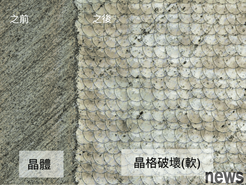
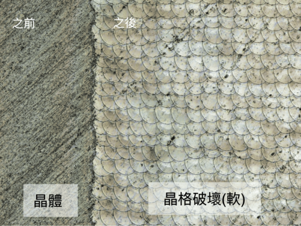
To solve this problem, the National Center of the National Research Institute and Dingni Technology cooperated to successfully introduce the Red External-line Nanosecond-level laser system, and developed a "laser grinding technology" designed for the mass production requirements of silicon carbide wafers. Through 100,000 strikes per second, the silicon carbide surface layer can be softened, and the grinding time of each wafer can be shortened from 3 hours to 2 hours without damaging the wafer. The wafer chip rate drops from 5% to 1%, greatly improving product yield, mainly improving the two-stage process of wafer grinding/spraying, wafer thinning and cutting.
The new technology can reduce the wafer consumption caused by the grinding process, and also clearly reduce the cost of cleaning and maintenance of consumables required for traditional grinding (diamond sand wheels, water, oil, etc.) and machine stations. The cost of bare wafer grinding consumables has dropped from US$23 to US$0.1, while avoiding the diamond particles used in mechanical grinding from being clamped by China, the main source of China.
The National Research Institute further pointed out that the new technology has another advantage, which can reduce the hardness of the silicon carbide wafer from the original 3000 HV to 60 HV, greatly reducing the subsequent processing time and cost.
Currently, Dingen Technology has cooperated with the Czech factory of the American chip manufacturer ON Semiconductor Corp. to prepare to promote its machine station to Europe.
Recommend News
-
Designed for the demand for silicon carbide wafers, China Research Institute coo
-

Ximen launches new smart verification solutions to accelerate verification proce
-

Taiwan s tax 20% has caused three major shocks! The Ministry of Economic Affairs
-

iPhone 17 news has been reversing again: the basic model will be equipped with A